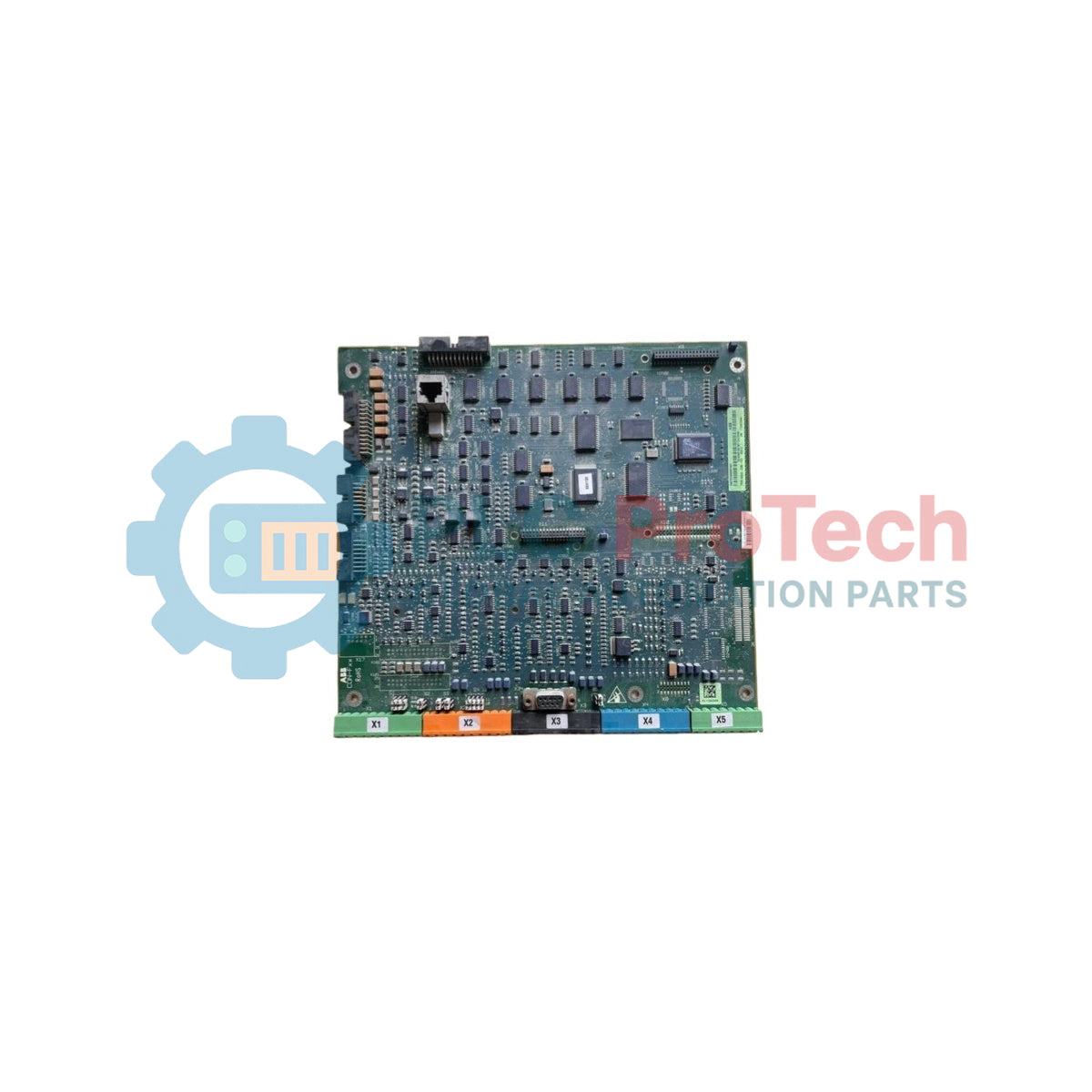
Description
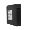
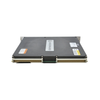
The ABB SDCS-CON-F01 is a centralized microprocessor main processing architecture engineered for the computational loops of DCS550 series DC drive systems. Operating as the primary control board, this card handles computational speed and torque calculation profiles, gating vector configurations, and field communication synchronization interfaces.
The SDCS-CON-F01 coordinates integrated peripheral commands through specialized onboards multi-channel interface links to drive scaling elements. This modular assembly, designated under product identifier 3ADT316500R1501, handles synchronous digital and analog processing infrastructure, preserving loop calculation integrity during fast-response thermal and armature power transitions in compact industrial networks.
Features
-
Centralized Processor Core: Manages real-time regulation loops for speed, torque, and current parameters within the drive chassis.
-
Direct Peripheral Mapping: Integrates connection lanes for encoder feedback tracking, pulse transformer interfaces, and optional extension modules.
-
Standard Firmware Path: Hosts high-density system logic memory to ensure predictable operational control parameters under variable loads.
-
Rigid Structural Mount: Formulated to bolt into internal drive swing frames, providing mechanical stability against heavy industrial panel vibrations.
Applications
- Main controller replacement inside multi-range modular units of the ABB DCS550 converter series.
- Variable speed DC motor power applications including plastic extruders, wire drawing machines, and conveyor control loops.
Technical Specifications
| Parameter |
Specification |
| Manufacturer |
ABB |
| Model Designation |
SDCS-CON-F01 |
| Product ID / Order Number |
3ADT316500R1501 |
| Drive Compatibility |
DCS550 Series DC Drives |
| Customs Tariff Number |
85371098 |
| Part Type Status |
Original / New |
| Product Net Weight |
0.399 kg |
| Shipping Weight (Calculated) |
0.650 kg |
| Package Dimensions (Calculated) |
260 mm x 180 mm x 45 mm |
Empirical Engineering Insights
Alternative Models & Compatibility
The SDCS-CON-F01 card is engineered strictly for the DCS550 drive environment and cannot be cross-swapped into older legacy DCS500 or larger DCS800 architectures due to dimensional layout variances and processing chip distinctions. When performing an on-site swap, ensure that your existing application parameters are saved via the drive configuration software before removing the faulty unit, as the replacement board requires complete parameters downloading to map your field infrastructure correctly.
Application Pitfalls & Engineering Notes
In high-temperature or non-ventilated electrical bays, inadequate heat convection can cause systemic computational issues inside the processor chip. Ensure enclosure cooling fans are functional. Additionally, ensure all flat ribbon data lines to the gating modules are fully seated; unsecured connectors can lead to firing phase imbalances, triggering immediate armature overcurrent faults or erratic tachometer readings during start-up.
Commissioning & Wiring Tips
Keep all low-voltage signal wiring lanes connected to the board terminals physically isolated from any parallel high-amperage AC feed tracks or motor armature lines to prevent electromagnetic noise coupling. Grounding tabs on the frame must maintain unpainted, raw metal-to-metal contact with the enclosure panel chassis to establish an absolute zero-potential reference plane and stabilize internal analog calculation tracks.
Installation Guidelines
CRITICAL WARNING: INDUSTRIAL POWER ISOLATION PROTOCOLS
Completely disconnect all main incoming line network paths, field excitation potentials, and external auxiliary supplies connected to the drive housing. DC converter topologies retain high voltage levels across electronic components after external breaker disconnection. Wait at least 15 minutes for internal filter circuits to discharge fully, and verify a safe zero-voltage state with a calibrated meter before exposing component frames.
1
Fasten a verified electrostatic discharge (ESD) wrist strap to local control cabinet ground to safeguard delicate onboard microprocessors.
2
Carefully extract the interface plugs, encoder terminal wires, and internal flat data ribbon loops from the card headers, recording layout coordinates.
3
Unscrew the structural board mounting points, fit the replacement unit securely into the chassis frame, and land all signal connectors firmly.