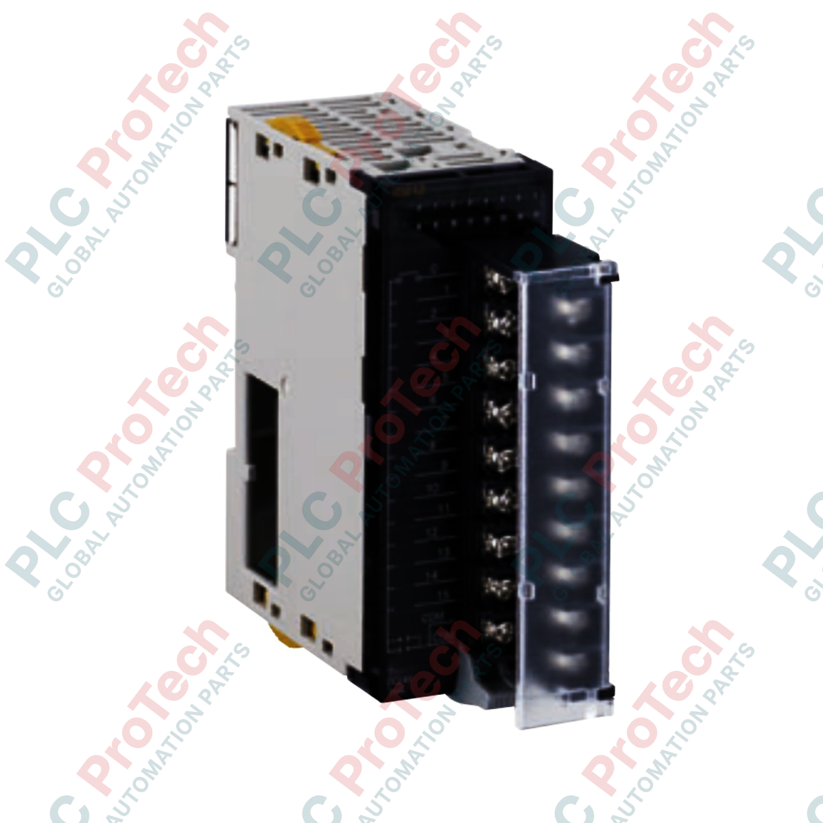
Description
Executing high-speed switching operations across complex control networks, the Omron CJ1W-OD213 functions as a reliable sinking transistor output module within the CJ-series PLC architecture. This module provides 16 discrete sinking output points on a single common terminal circuit, engineered specifically to handle precision high-frequency switching tasks with an ultra-fast response envelope of 15 microseconds for ON transitions and 80 microseconds for OFF transitions. Its space-saving design integrates directly onto the standard CJ-series backplane and features a detachable terminal block to simplify field wiring and routine maintenance without disturbing system connections.
Features
-
High-Speed Switching: Outstanding transient response times (15 us ON max, 80 us OFF max) optimize its performance in fast-cycle machine control.
-
Efficient Channel Density: 16 sinking transistor outputs grouped into a single circuit to minimize module footprint on the chassis.
-
Robust Load Capacity: Supports individual loads of up to 0.5 A per point while maintaining a combined unit capacity of up to 5.0 A.
-
Detachable Terminal Block: Enables pre-wiring and swap-out of module electronics without disconnecting external field wires.
-
Clear Diagnostic Indicators: Front-facing LED status lights show the active operational status of each individual output point.
Applications
-
Solenoid Valve Control: Driving low-power pneumatic and hydraulic directional valves on automated production lines.
-
Packaging Machinery: Operating indexing mechanisms, pushers, and high-speed labeling heads.
-
Semiconductor Processing: Controlling auxiliary material handling, cleaning cycles, and transfer systems.
-
Discrete Assembly Systems: Managing light curtains, tower lights, small relays, and electronic actuators.
Technical Specifications
| Parameter |
Value |
| Manufacturer |
Omron |
| Model Number |
CJ1W-OD213 |
| Module Type |
Transistor Output Unit (Sinking Outputs) |
| Number of Output Points |
16 points (16 points/common, 1 circuit) |
| Rated Load Voltage |
24 VDC |
| Operating Load Voltage Range |
20.4 to 26.4 VDC |
| Maximum Load Current |
0.5 A per point, 5.0 A per unit |
| Maximum Inrush Current |
4.0 A per point, 10 ms maximum |
| Leakage Current |
0.1 mA maximum |
| Residual Voltage |
1.5 V maximum |
| ON Response Time |
15 microseconds maximum |
| OFF Response Time |
80 microseconds maximum |
| Insulation Resistance |
20 MOhm minimum between external terminals and GR terminal (at 100 VDC) |
| Dielectric Strength |
1,000 VAC between external terminals and GR terminal for 1 minute (leakage current: 10 mA max) |
| Internal Current Consumption |
150 mA maximum at 5 VDC |
| External Power Supply Requirements |
20.4 to 26.4 VDC, 55 mA minimum |
| Fuses |
None (external fusing recommended) |
| Module Net Weight |
110 g maximum |
| Shipping Weight (Calculated) |
1.2 kg |
Connections and Interfaces
This sinking output module relies on an external 24 VDC power source to switch the field loads. Ensure proper polarity is observed during terminal wiring to prevent circuit damage.
| Terminal Point |
Signal Function |
Wiring Detail |
| 0 to 15 |
Output Channels 00 to 15 |
Connect to individual load negative sides (sinking load path) |
| COM |
Sinking Output Common |
Connected to the 0 VDC side of the external load supply |
| +V |
External Power Supply Input (+V) |
Connect to +24 VDC side of the external load supply (required for internal drive logic) |
Empirical Engineering Insights
Alternative Models & Compatibility
When updating legacy machinery, note that this module uses a detachable M3 screw terminal block for connection. It is often evaluated as a modular alternative to high-density models like the CJ1W-OD231, which uses a 40-pin connector layout. Moving from connector-style modules to terminal-block units requires verifying the physical enclosure wireways and spacing constraints.
Application Pitfalls & Engineering Notes
Because this module is designed without built-in internal fuses, any high-current short on an output channel will permanently destroy the associated output transistor. It is critical to incorporate fast-acting external fuses in series with the load supply line to safeguard the internal backplane circuitry. Furthermore, while individual channels support 0.5 A, the aggregate current limit of 5.0 A must not be exceeded under continuous operation across all active channels.
Commissioning & Wiring Tips
Always implement inductive surge suppression diodes in parallel with inductive loads, such as relay coils or solenoid valves. Transistor outputs are highly sensitive to back-EMF spikes generated upon de-energizing inductive loads; failing to install snubber diodes close to the load can lead to pre-mature channel failure or intermittent backplane communication resets.
Installation Guidelines
CRITICAL WARNING
Isolate and lock out all power sources (both the main PLC system and external output load supplies) before mounting, dismounting, or servicing terminal connections. Failure to remove external power before working on the module can result in equipment damage, accidental actuator activation, or electrical shock.
1
Hook the top bracket of the module onto the slot of the CJ-series backplane and pivot the module securely into position until it snaps flush with the bus connection.
2
Tighten the upper and lower mounting screws to lock the physical module firmly to the backplane, ensuring proper chassis grounding and resistance to vibration.
3
Wire the field devices to the detached terminal block according to the sinking output electrical schematic, and secure the +24 VDC external drive voltage lines.
4
Align and press the completed terminal block firmly into the module until the locking tabs snap shut, verifying clear LED visualization pathways.